Credit: CFP
TMTPOST -- China has taken a major step forward in semiconductor technology with the development of its first domestically produced commercial electron beam lithography (EBL) machine, “Xizhi,” which has now entered the application testing phase, Hangzhou Daily reported Thursday.
The development represents a critical leap forward in China’s quantum chip research and development capabilities, providing a domestically produced precision tool on par with mainstream international equipment.
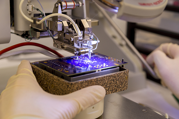
The “Xizhi” lithography machine, independently developed by Zhejiang University’s Yuhang Quantum Research Institute, is capable of achieving 0.6-nanometer accuracy and line widths of 8 nanometers, enabling highly precise circuit writing essential for advanced quantum chip fabrication. “This is not an ordinary machine; it is a ‘nano-pen’ capable of engraving an entire city map on a strand of hair,” a representative of the research team said, highlighting the machine’s extraordinary precision.
Resembling a large steel cabinet, the “Xizhi” uses a high-energy electron beam to “write” circuits directly onto silicon wafers. Unlike traditional photolithography, which requires costly photomasks, EBL allows flexible design changes—an advantage especially valuable during the iterative development phases of quantum chips. Researchers can make rapid adjustments to circuit patterns without being constrained by mask fabrication, significantly accelerating early-stage experimentation.
The machine’s development also addresses long-standing challenges posed by international export restrictions. For years, Chinese research institutions and companies, including the University of Science and Technology of China and Zhejiang Lab, faced barriers to accessing high-end lithography tools due to export controls. “The commercialization of ‘Xizhi’ not only fills this domestic gap but also establishes a complete domestic replacement chain,” the team representative noted. The machine is now positioned to support both fundamental research and applied quantum chip manufacturing in China.

Named after the celebrated Chinese calligrapher Wang Xizhi, the machine’s designation reflects the precision and delicacy of traditional calligraphy applied at the nanoscale. “Our ‘brush’ is the electron beam, which writes circuits on chips,” the representative said, emphasizing the technological artistry embedded in the design. The analogy underscores how the machine can execute highly detailed and repeatable patterns, essential for debugging and testing in quantum chip development.
The introduction of “Xizhi” is expected to enhance China’s competitiveness in high-end manufacturing and scientific research. Its applications extend beyond quantum chips to broader semiconductor R&D, potentially catalyzing advances in AI, photonics, and other frontier technologies. By providing an indigenous platform for iterative experimentation and production, the machine supports the country’s goal of technological self-reliance in critical semiconductor processes.
Experts note that the “Xizhi” machine’s launch also strengthens China’s position within the global semiconductor supply chain. With the machine entering the market, domestic manufacturers and research institutions can reduce dependency on foreign suppliers, ensuring that strategic advancements in quantum chip development remain largely in-country. The project also signals China’s commitment to converting scientific achievements into industrial productivity, a priority for national technological competitiveness.
“The testing phase of ‘Xizhi’ is a significant milestone,” said an industry expert. “It demonstrates that China can now develop, produce, and deploy high-precision lithography tools independently. This capability will be crucial in maintaining leadership in quantum chip R&D and advancing the country’s broader semiconductor ambitions.”
As China continues to invest in cutting-edge semiconductor technologies, the Xizhi electron beam lithography machine exemplifies the country’s drive toward innovation, precision manufacturing, and technological self-sufficiency. Its successful deployment may well accelerate China’s transition from scientific experimentation to industrial-scale production in quantum and advanced chip technologies, further solidifying its role in the global semiconductor industry.
更多精彩内容,关注钛媒体微信号(ID:taimeiti),或者下载钛媒体App