For the past several weeks, headlines have been screaming about the looming threat and potential impact of U.S. import tariffs being imposed on semiconductors. Truthfully, I don’t think implementation of these tariffs will ever happen because they would result in such significant supply chain disruption, the nasty effects of which are still all too fresh in our memories from COVID-19. Who can forget the tens of thousands of unfinished cars left stranded in automotive manufacturers’ lots. Certainly, no one wants a repeat of that!
That said, I believe it still behooves U.S. businesses and the U.S. economy overall to become more resilient and self-reliant in the area of semiconductor manufacturing, and I applaud these efforts. Here, we’ll examine why this self-reliance is so important, particularly in terms of the U.S.’s ability to maintain its (currently narrow) leadership in state-of-the art artificial intelligence (AI).
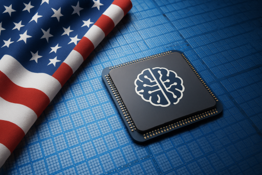
The AI Race Is, At its Core, A Chips Race
Semiconductors are crucial for powering the servers that train AI models, as training these models requires a specialized strength that only semiconductors (versus traditional processors) can deliver. It’s estimated that by the end of this year, AI-related semiconductors will account for 19 percent of the total semiconductor market worldwide, a significant increase from the seven percent held in 2017.
Increased reliance on semiconductors for AI means the less the U.S. relies on foreign entities for semiconductor supply, the better. As the global AI race heats up, domestic semiconductor production offers significant benefits like bolstered economic and national security, as well as technological independence. Currently, there’s a bill passing through Congress called the “Securing Semiconductor Supply Chains Act of 2025,” which has bipartisan support and is aimed squarely at reducing reliance on unpredictable foreign supply chains.
How Do We Do It?
In response to the threat of possible U.S. import tariffs, many have voiced concerns that in its current state, the U.S. is ill-equipped to handle the skyrocketing semiconductor demand being driven by generative AI and AI datacenter build-outs. Business uses of AI, such as coding and software development, are especially at risk. Any disruption in semiconductor access could induce a ripple effect across dependent application areas, including AI and downstream markets like autonomous vehicles, edge computing and robotics.
The U.S.’s ability to drive innovation across semiconductor-dependent industries, including AI, will require an acceleration of materials discovery. The “old way” of materials discovery and adoption was typically concentrated in overseas foundries and involved multi-step processes like photolithography, etching, deposition and clean rooms. This can be a slow and expensive process, leading to lengthy design cycles and significant materials waste.
To better meet semiconductor demand domestically, the U.S. must take advantage of advancements in chip design, one technique being direct local atomic layer processing. This is a digital, atomically precise manufacturing process that builds devices directly from atoms, eliminating the need for the many steps involved in the traditional manufacturing process, while reducing complexity and waste. It offers unprecedented flexibility and precision for designing and prototyping a wide variety of microdevices, including AI semiconductors.
By enabling atomic-scale precision and control over materials processing, technologies like direct local atomic layer processing can significantly accelerate design cycles and prototyping, helping to find new materials or combinations of materials that can satisfy the ever-growing compute needs of AI.
Increasing Domestic Manufacturing While Remaining Committed to Environmental and Human Health
As an additional (and not inconsequential) benefit, new techniques can also dramatically lessen the environmental impact of semiconductor manufacturing. To date, this industry has faced a serious dilemma due to its outsized environmental footprint, contributing significantly to greenhouse gas emissions, water consumption and chemical waste, particularly toxic ‘forever chemicals’ known as PFAS. These are chemicals which pollute water, do not break down and remain in the environment (and in people!) for decades.
It’s no wonder that recent federal actions like the Building Chips in America Act and the CHIPS Act have raised significant environmental concerns. By slashing the time needed to design, prototype and manufacture chips – and eliminating the need for chemical-intensive clean-room environments – new techniques can be the answer to satisfying demand and scaling responsibly using domestic resources, and without compromising environmental and human health.
Harnessing the U.S.’s Collective Resources
In addition to deploying new manufacturing techniques, the U.S. must update its overall approach. This means moving away from a model of heavily offshoring production to a small handful of multi-billion dollar foundries, to leveraging the nation’s comprehensive and rich arsenal of leading universities, startups and industrial R&D firms to collaborate, accelerate discovery and support the entire ‘lab-to-fab’ process (research, prototyping and manufacturing). This can all be achieved while keeping costs in check and integrating enabling technologies directly into these organizations’ infrastructures.
Looking Ahead
The relationship between AI and semiconductors is truly symbiotic. As we’ve mentioned, semiconductors are crucial for powering the servers that train AI models; on the flipside, AI is significantly accelerating semiconductor materials discovery by leveraging machine learning to predict the properties of new materials and accelerate the design process. This approach, known as inverse materials design, allows researchers to design materials with specific targeted properties, such as improved conductivity, energy efficiency and sustainability.
Accelerating the discovery of new materials remains one of the toughest challenges in semiconductor manufacturing, though it’s particularly demanding for AI semiconductors, as the industry seeks to constantly drive up computational power, efficiency and speed, while reducing chip size.
While AI can be used to predict the properties of new, theoretical materials, these breakthroughs have traditionally still been limited by the slow pace of physical validation. New techniques can be used to support high-throughput experimentation, helping to close the gap; enabling faster, more targeted materials development, and ultimately unlocking the next generation of materials. Combining new techniques like direct atomic layer processing with the power of AI has the power to make magic, dramatically accelerating the development of breakthroughs that were never before thought to be possible, all centralized within the U.S.’ own national borders.
The post Strengthening U.S. Chip Manufacturing – The Key to AI Leadership appeared first on Unite.AI.