Everyday life is three dimensional, with even a sheet of paper having a finite thickness. Shengxi Huang from Rice University in the US, however, is attracted by 2D materials, which are usually just one atomic layer thick. Graphene is perhaps the most famous example — a single layer of carbon atoms arranged in a hexagonal lattice. But since it was first created in 2004, all sorts of other 2D materials, notably boron nitride, have been created.
An electrical engineer by training, Huang did a PhD at the Massachusetts Institute of Technology and postdoctoral research at Stanford University before spending five years as an assistant professor at the Pennsylvania State University. Huang has been at Rice since 2022, where she is now an associate professor in the Department of Electrical and Computer Engineering, the Department of Material Science and NanoEngineering, and the Department of Bioengineering.
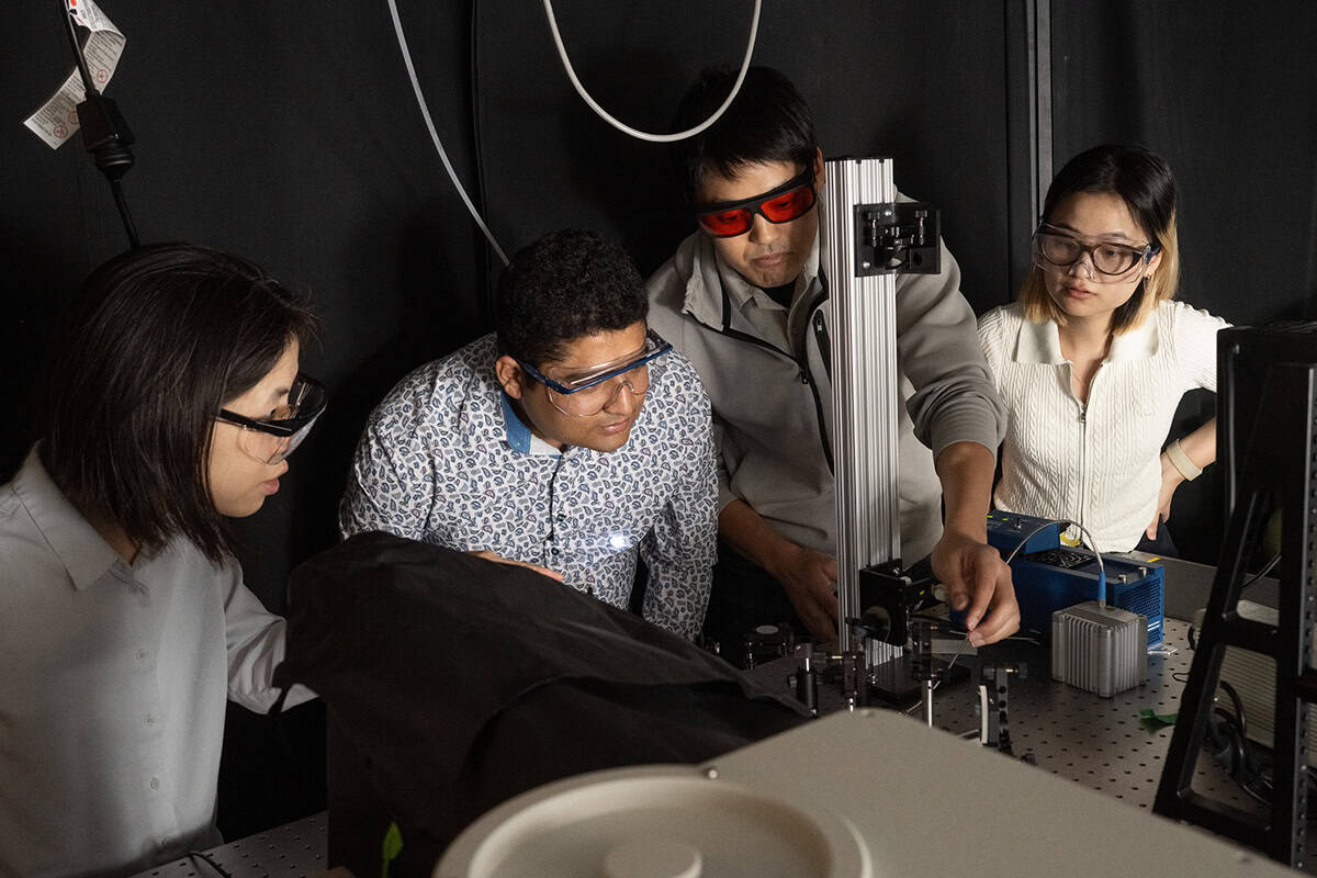
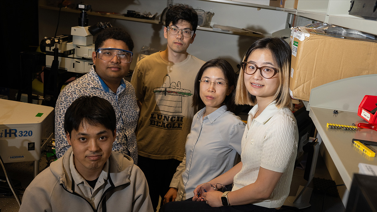
Her group at Rice currently has 12 people, including eight graduate students and four postdocs. Some are physicists, some are engineers, while others have backgrounds in material science or chemistry. But they all share an interest in understanding the optical and electronic properties of quantum materials and seeing how they can be used, for example, as biochemical sensors. Lab equipment from Picoquant is vital in helping in that quest, as Huang explains in an interview with Physics World.
Why are you fascinated by 2D materials?
I’m an electrical engineer by training, which is a very broad field. Some electrical engineers focus on things like communication and computing, but others, like myself, are more interested in how we can use fundamental physics to build useful devices, such as semiconductor chips. I’m particularly interested in using 2D materials for optoelectronic devices and as single-photon emitters.
What kinds of 2D materials do you study?
The materials I am particularly interested in are transition metal dichalcogenides, which consist of a layer of transition-metal atoms sandwiched between two layers of chalcogen atoms – sulphur, selenium or tellurium. One of the most common examples is molybdenum disulphide, which in its monolayer form has a layer of sulphur on either side of a layer of molybdenum. In multi-layer molybdenum disulphide, the van der Waals forces between the tri-layers are relatively weak, meaning that the material is widely used as a lubricant – just like graphite, which is a many-layer version of graphene.
Why do you find transition-metal dichalcogenides interesting?
Transition metal dichalcogenides have some very useful optoelectronic properties. In particular, they emit light whenever the electron and hole that make up an “exciton” recombine. Now because these dichalcogenides are so thin, most of the light they emit can be used. In a 3D material, in contrast, most light is generated deep in the bulk of the material and doesn’t penetrate beyond the surface. Such 2D materials are therefore very efficient and, what’s more, can be easily integrated onto chip-based devices such as waveguides and cavities.
Transition metal dichalcogenide materials also have promising electronic applications, particularly as the active material in transistors. Over the years, we’ve seen silicon-based transistors get smaller and smaller as we’ve followed Moore’s law, but we’re rapidly reaching a limit where we can’t shrink them any further, partly because the electrons in very thin layers of silicon move so slowly. In 2D transition metal dichalcogenides, in contrast, the electron mobility can actually be higher than in silicon of the same thickness, making them a promising material for future transistor applications.
What can such sources of single photons be used for?
Single photons are useful for quantum communication and quantum cryptography. Carrying information as zero and one, they basically function as a qubit, providing a very secure communication channel. Single photons are also interesting for quantum sensing and even quantum computing. But it’s vital that you have a highly pure source of photons. You don’t want them mixed up with “classical photons”, which — like those from the Sun — are emitted in bunches as otherwise the tasks you’re trying to perform cannot be completed.
What approaches are you taking to improve 2D materials as single-photon emitters?
What we do is introduce atomic defects into a 2D material to give it optical properties that are different to what you’d get in the bulk. There are several ways of doing this. One is to irradiate a sample with ions or electrons, which can bombard individual atoms out to generate “vacancy defects”. Another option is to use plasmas, whereby atoms in the sample get replaced by atoms from the plasma.
So how do you study the samples?
We can probe defect emission using a technique called photoluminescence, which basically involves shining a laser beam onto the material. The laser excites electrons from the ground state to an excited state, prompting them to emit light. As the laser beam is about 500-1000 nm in diameter, we can see single photon emission from an individual defect if the defect density is suitable.
What sort of experiments do you do in your lab?
We start by engineering our materials at the atomic level to introduce the correct type of defect. We also try to strain the material, which can increase how many single photons are emitted at a time. Once we’ve confirmed we’ve got the correct defects in the correct location, we check the material is emitting single photons by carrying out optical measurements, such as photoluminescence. Finally, we characterize the purity of our single photons – ideally, they shouldn’t be mixed up with classical photons but in reality, you never have a 100% pure source. As single photons are emitted one at a time, they have different statistical characteristics to classical light. We also check the brightness and lifetime of the source, the efficiency, how stable it is, and if the photons are polarized. In fact, we have a feedback loop: what improvements can we do at the atomic level to get the properties we’re after?
Is it difficult adding defects to a sample?
It’s pretty challenging. You want to add just one defect to an area that might be just one micron square so you have to control the atomic structure very finely. It’s made harder because 2D materials are atomically thin and very fragile. So if you don’t do the engineering correctly, you may accidentally introduce other types of defects that you don’t want, which will alter the defects’ emission.
What techniques do you use to confirm the defects are in the right place?
Because the defect concentration is so low, we cannot use methods that are typically used to characterise materials, such as X-ray photo-emission spectroscopy or scanning electron microscopy. Instead, the best and most practical way is to see if the defects generate the correct type of optical emission predicted by theory. But even that is challenging because our calculations, which we work on with computational groups, might not be completely accurate.
How do your PicoQuant instruments help in that regard?
We have two main pieces of equipment – a MicroTime 100 photoluminescence microscope and a FluoTime 300 spectrometer. These have been customized to form a Hanbury Brown Twiss interferometer, which measures the purity of a single photon source. We also use the microscope and spectrometer to characterise photoluminescence spectrum and lifetime. Essentially, if the material emits light, we can then work out how long it takes before the emission dies down.
Did you buy the equipment off-the-shelf?
It’s more of a customised instrument with different components – lasers, microscopes, detectors and so on — connected together so we can do multiple types of measurement. I put in a request to Picoquant, who discussed my requirements with me to work out how to meet my needs. The equipment has been very important for our studies as we can carry out high-throughput measurements over and over again. We’ve tailored it for our own research purposes basically.
So how good are your samples?
The best single-photon source that we currently work with is boron nitride, which has a single-photon purity of 98.5% at room temperature. In other words, for every 200 photons only three are classical. With transition-metal dichalcogenides, we get a purity of 98.3% at cryogenic temperatures.
What are your next steps?
There’s still lots to explore in terms of making better single-photon emitters and learning how to control them at different wavelengths. We also want to see if these materials can be used as high-quality quantum sensors. In some cases, if we have the right types of atomic defects, we get a high-quality source of single photons, which we can then entangle with their spin. The emitters can therefore monitor the local magnetic environment with better performance than is possible with classical sensing methods.
- More information about the author’s work can be found in ACS Nano (16 7428) and J. Phys. Chem. Lett. (14 3274).
![]()
The post Shengxi Huang: how defects can boost 2D materials as single-photon emitters appeared first on Physics World.