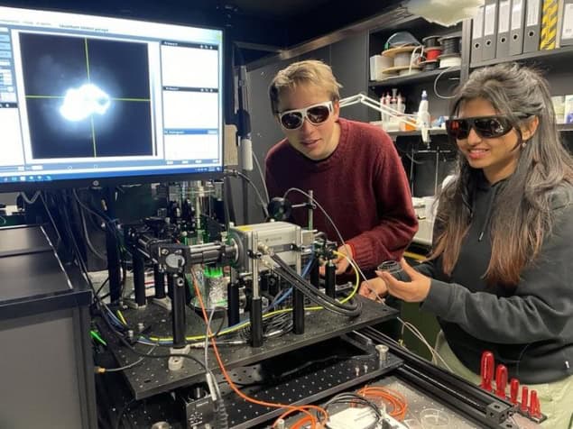
A newly discovered carbon-based defect in the two-dimensional material hexagonal boron nitride (hBN) could be used as a quantum sensor to detect magnetic fields in any direction – a feat that is not possible with existing quantum sensing devices. Developed by a research team in Australia, the sensor can also detect temperature changes in a sample using the boron vacancy defect present in hBN. And thanks to its atomically thin structure, the sensor can conform to the shape of a sample, making it useful for probing structures that aren’t perfectly smooth.
The most sensitive magnetic field detectors available today exploit quantum effects to map the presence of extremely weak fields. To date, most of these have been made out of diamond and rely on the nitrogen vacancy (NV–) centres contained within. NV– centres are naturally occurring defects in the diamond lattice in which two carbon atoms are replaced with a single nitrogen atom, leaving one lattice site vacant. Together, the nitrogen atom and the vacancy can behave as a negatively charged entity with an intrinsic spin. NV– centres are isolated from their surroundings, which means that their quantum behaviour is robust and stable.
When a photon hits an NV– centre, it can excite an electron to a higher-energy state. As it then decays back to the ground state, it may emit a photon of a different wavelength. The NV– centre has three spin sublevels, and the excited state of each sublevel has a different probability of emitting a photon when it decays.
By exciting an individual NV– centre repeatedly and collecting the emitted photons, researchers can detect its spin state. And since the spin state can be influenced by external variables such as magnetic field, electric field, temperature, force and pressure, NV– centres can therefore be used as atomic-scale sensors. Indeed, they are routinely employed today to study a wide variety of biological and physical systems.
There is a problem though – NV– centres can only detect magnetic fields that are aligned in the same direction as the sensors. Devices must therefore contain many sensors placed at different alignment angles, which makes them difficult to use and limited to specific applications. What’s more, the fact that they are rigid (diamond being the hardest material known), means they cannot conform to the sample being studied.
A new carbon-based defect
Researchers recently discovered a new carbon-based defect in hBN, in addition to the boron vacancy that it is already known to contain. In this latest work, and thanks to a carefully calibrated Rabi experiment (a method for measuring nuclear spin), a team led by Jean-Philippe Tetienne of RMIT University and Igor Aharonovich of the University of Technology Sydney found that the carbon-based defect behaves as a spin-half system (S=1/2). In comparison, the spin in the boron defect is equal to one. And it’s this spin-half nature of the former that enables it to detect magnetic fields in any direction, say the researchers.

“Having two different independently addressable spin species within the same material at room temperature is unique, not even diamond has this capability,” explains Priya Singh from RMIT University, one of the lead authors of this study. “This is exciting because each spin species has its advantages and limitations, and so with hBN we can combine the best of both worlds. This is important especially for quantum sensing, where the spin half enables omnidirectional magnetometry, with no blind spot, while the spin one provides directional information when needed and is also a good temperature sensor.”
Until now, the spin multiplicity of the carbon defect was under debate in the hBN community, adds co-first author Sam Scholten from the University of Melbourne. “We have been able to unambiguously prove its spin-half nature, or more likely a pair of weakly coupled spin-half electrons.”
The new S=1/2 sensor can be controlled using light in the same way as the boron vacancy-based sensor. What’s more, the two defects can be tuned to interact with each other and thus used together to detect both magnetic fields and temperature at the same time. Singh points out that the carbon-based defects were also naturally present in pretty much every hBN sample the team studied, from commercially sourced bulk crystals and powders to lab-made epitaxial films. “To create the boron vacancy defects in the same sample, we had to perform just one extra step, namely irradiating the samples with high-energy electrons, and that’s it,” she explains.
To create the hBN sensor, the researchers simply drop casted a hBN powder suspension onto the target object or transferred an epitaxial film or an exfoliated flake. “hBN is very versatile and easy to work with,” says Singh. “It is also low cost and easy to integrate with various other materials so we expect lots of applications will emerge in nanoscale sensing – especially thanks to the omnidirectional magnetometry capability, unique for solid-state quantum sensors.”
The researchers are now trying to determine the exact crystallographic structure of the S=1/2 carbon defects and how they can engineer them on-demand in a few layers of hBN. “We are also planning sensing experiments that leverage the omnidirectional magnetometry capability,” says Scholten. “For instance, we can now image the stray field from a van der Waals ferromagnet as a function of the azimuthal angle of the applied field. In this way, we can precisely determine the magnetic anisotropy, something that has been a challenge with other methods in the case of ultrathin materials.”
The study is detailed in Nature Communications.
The post Carbon defect in boron nitride creates first omnidirectional magnetometer appeared first on Physics World.

